HONEYSTONE
About us
Honeystone Ltd. supplies equipment for Thick Film hybrid technology and semiconductor packaging worldwide. Our qualified engineers provide installation, warranty, and lifetime maintenance support.
With strong engineering expertise, we offer cost-effective project assistance, technical consulting, and support during product development and proof-of-concept stages.
Across markets, we act as representatives and consultants for equipment and materials manufacturers, delivering application advice, sales, and full service throughout the asset's life cycle.
Chip Resistors
Turn Key manufacturing lines for high precision, high mix low-volume chip resistor production
Videos
Belt Furnaces from Hengli Eletek
Aurel standart product line
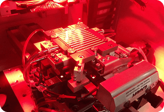
Thick Film Manufacture
Hengli 2025
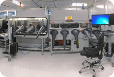
Our services
Turnkey production equipment supply and service worldwide Process development and Product design assistance
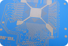
Thick Film Hybrids
Classic Thick Film
screen fabrication, printing, drying, firing, trimming, optical inspection, calibration, sorting, and environmental testing.
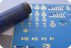
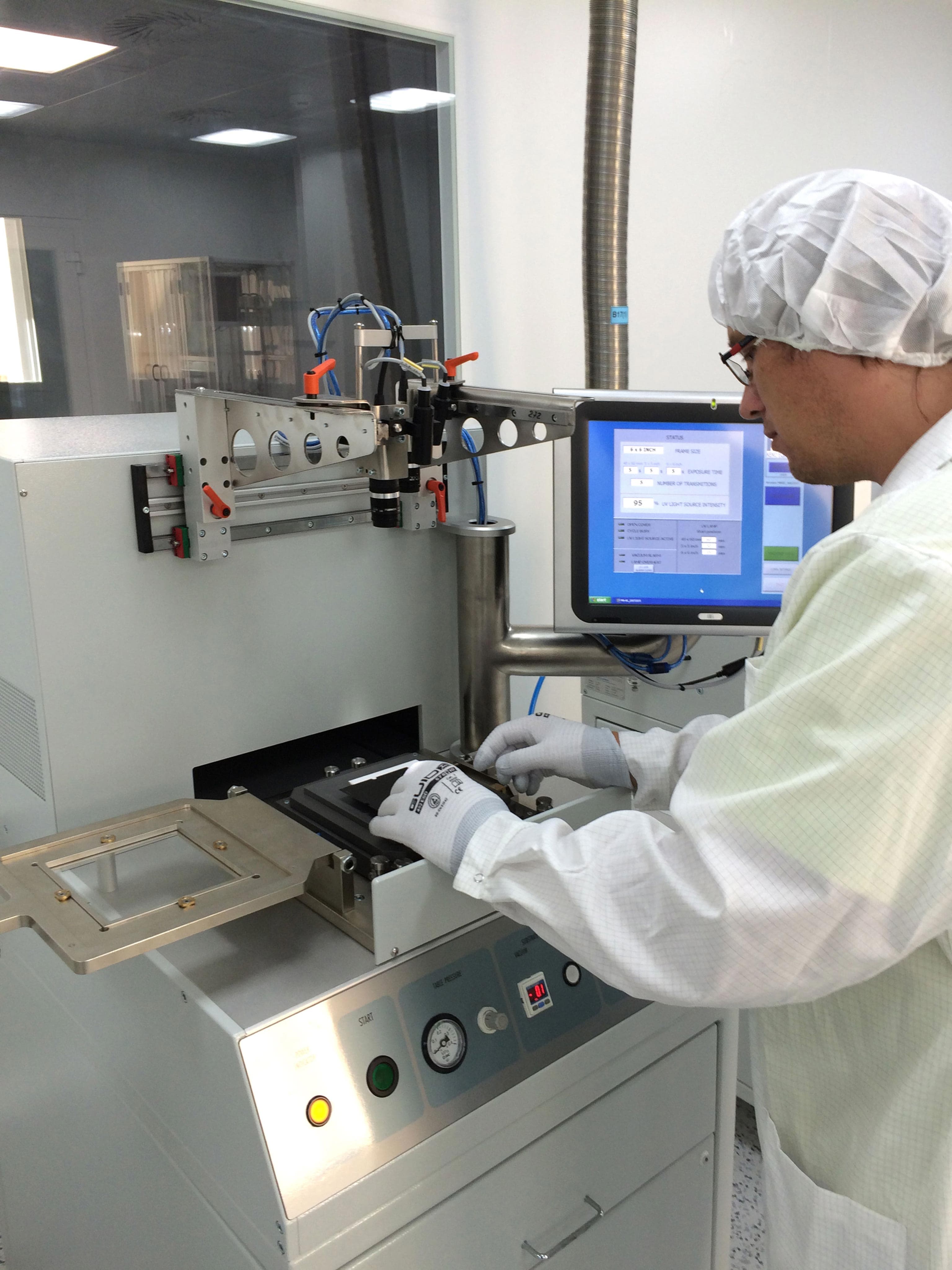
Fine Line Thick Film
use of photoimageable pastes, exposure, and development for precise circuit patterns.
Multilayer Ceramic Processes
processing, assembling, and sintering of complex multilayer electronic structures.
Heterogenous Structures, composites and batteries
Glass Feed-throughs GTMS/HTCC
glass-to-metal sealing, kovar ring and leadframe brazing and plating.
DBC/AMB Substrates
oxidation, sputtering, copper bonding, photolithography, etching, and plating for power electronics.
SOFC and Hydrolisers
Cell ink and ceramic slurry manufacturing, screen printing, dispensing or casting, stacking layers, hermetic sealing and the final assembly
Battery Active Materials
Milling, mixing and drying of cathode and anode materials, conveying and thermal treatment in calcination kilns, complete factory solutions for LFP Gen 3 and 4, MLFP, NCM, Sodium cathodes, graphite, composite Si-C and metal oxide anodes
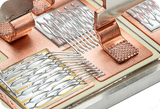
Back-End Advanced Packaging
Cutting, scribing, heat treatment (vacuum, inert or reducing gases).
Die bonding, microassembly, fluxless soldering.
Wire bonding, laser welding for high-power products.
Hermetic sealing of cases in a controlled atmosphere.
Forming cases on leadframes, testing (electrical, structural, environmental).
Our Recent Projects Worldwide

Chip Resistors
Turn Key manufacturing lines for high precision, high mix low-volume chip resistor production
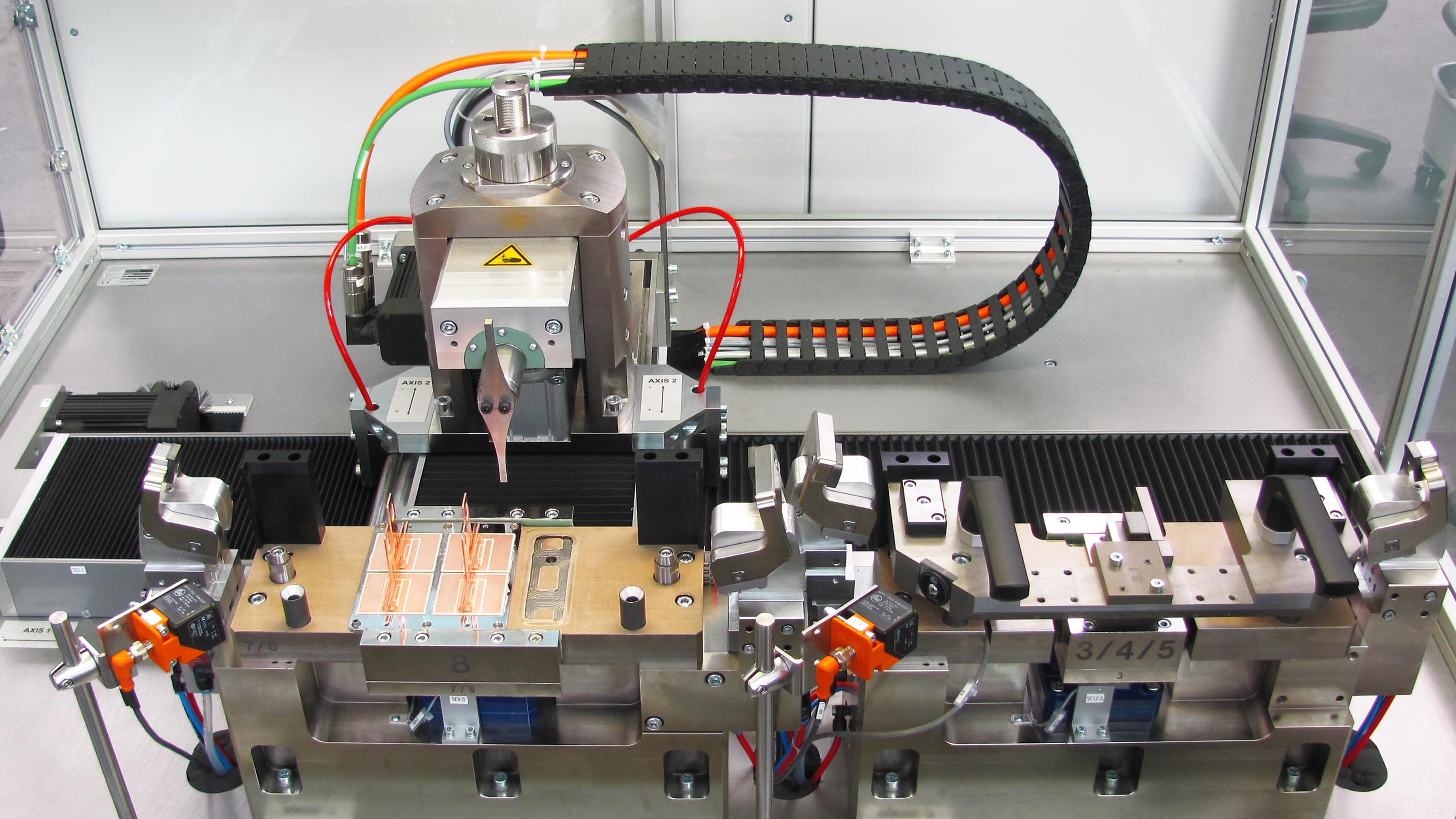
Power IGBT Modules
Turn Key mid-volume production and test facility
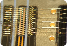
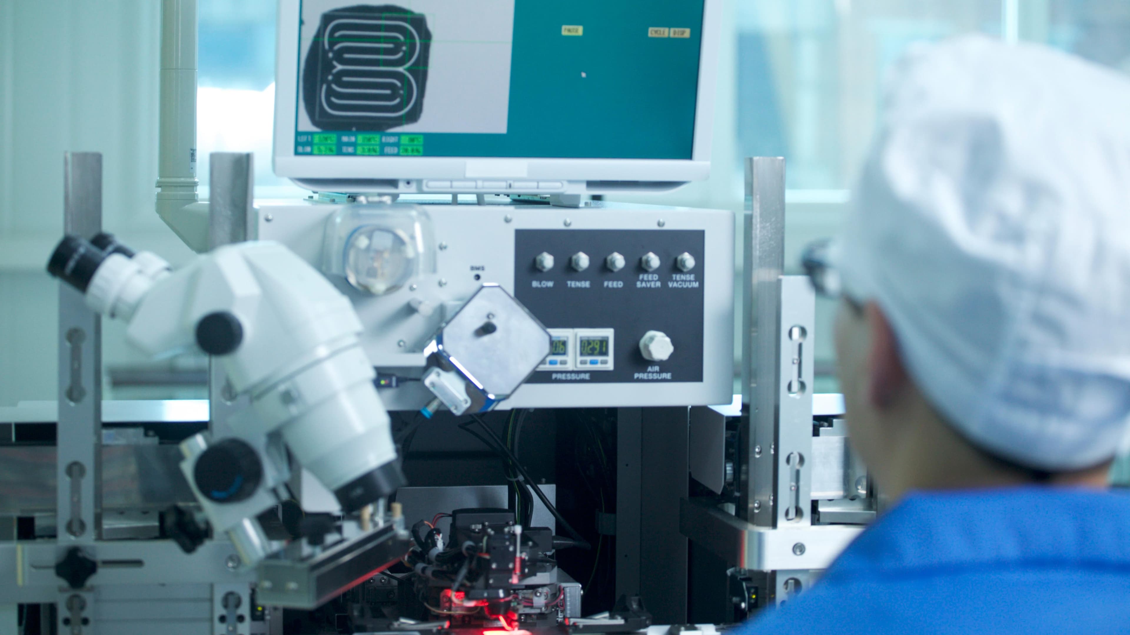
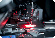
Wire Bonding Applications
Ball, Wedge, TAB and Ribbon bonding for ASICs, discretes, RF and power electronics
LED modules
SMT and Packaging Lines for a "Connected City" LED Streetlights network
Hermetic packages sealing
Complex production line with high vacuum outgassing, Parallel Seam and Laser welding stations and gas recirculation modules.
Fine Line Thick Film Hybrids
Turn Key solutions and process consulting for Thick Film fine line hybrids, including multilayers on fired and LTCC ceramics
LTCC and Hybrid Modules
Advanced Multichip LTCC Modules Production Line with Packaging and Test Facility
Training Programs
The unique proposition is our independent advice Operator and process technician training programs Process audits and Coached production at the Customer's facility.
Training Programs at affordable daily rate
Screen Manufacture Process
From frame and mesh selection to proper storage, step by step materials guide and process set up
Firing Furnace Set up
Air pressure and flow adjustment methods, temperature profiling and verification
Design Rules
Thick and Thin Film process limitations and pitfalls
Screen Printing
Up to 70% of defects can be eliminated by optimisation of screen printing parameters
Thick Film Process documentation
A set of Process Instructions in either paper or electronic interactive format based on ScanCAD ™ ProWorks ™ platform
Coached Production
New Product launch assistance, manufacturing of samples and production ramping up at the Customer's site
Our location
Honeystone Limited
Ground Floor,
123 Pall Mall SW1Y 5EA London UK
Follow the news in our
Linkedin profile